Hey everyone!
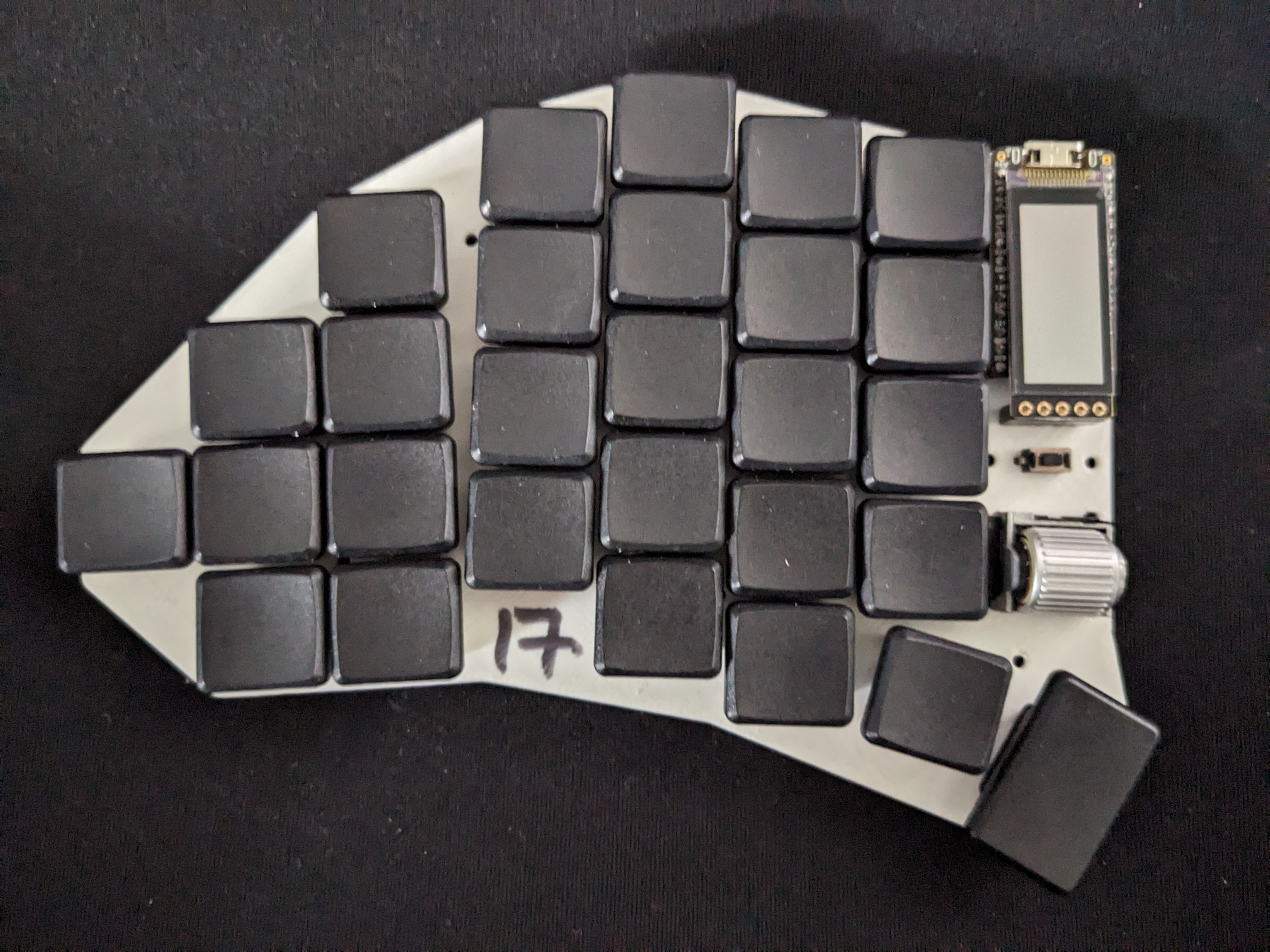
I jumped into the ergomech rabbit hole sometime last year and after using a sofle as my daily driver since then, I now decided it's time to build my own "thing". After going through endless revisions to figure out what I actually want, and trying to learn how to trace PCBs, this is what I have come up with: A choc-spaced 56 keys wireless build with a scrollwheel and some staggering.
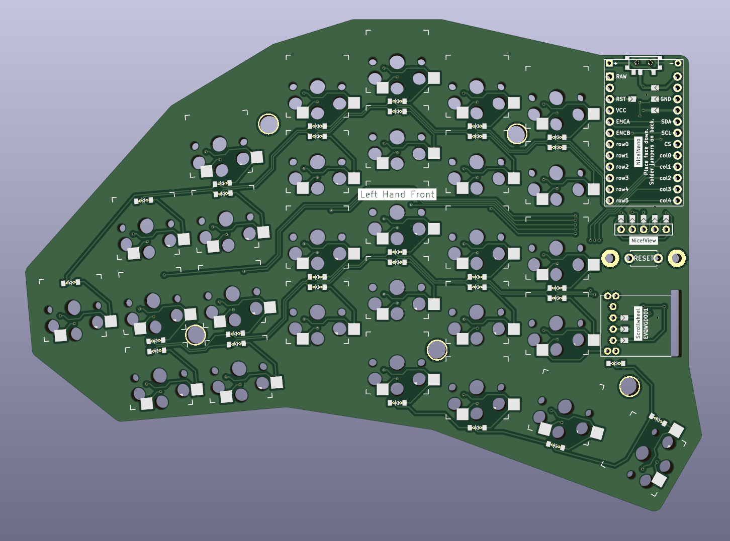
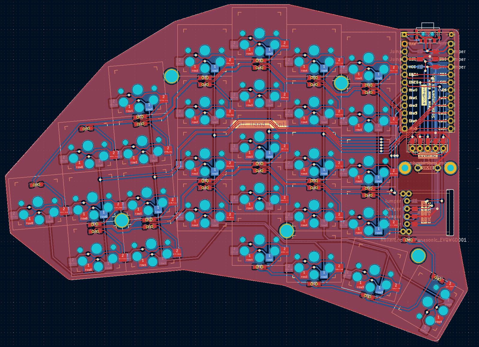
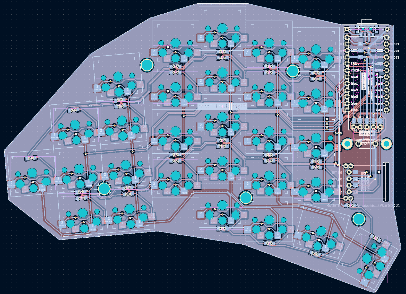
It's a reversible PCB. To make this work with single pin hole for both sides, I used jumpers for pins that can not be set in software (VCC, GND, RST). For rows/columns, I plan to do a different mapping in software to not have a jumper for every single pin.
All files including the kicad_pcb and ergogen config are available and open source at github: https://github.com/dnlbauer/splitkeyboard .
However, this is the first thing I ever designed. Therefore, I was hoping if you guys could have a look at the PCB before I get it etched and point out if there are any obvious errors?
Of course, I am also happy about any feedback in general. :)
13 Comments
Skree@lemmy.world · 3 pts · 3y
I'll give things a look over. First thought, you ground poured, but didn't link any of it together with vias. That would be helpful in ensuring good ground return paths.
Skree@lemmy.world · 3 pts · 3y
Yeah just some vias for return to ground; everything looks reasonably fine from a quick overview. You have space, and cross talk really isn't a concern, but more padding between signal traces could be helpful in some of the closer areas. Though all of that is minimal in concern.
dnl@lemmy.world · 2 pts · 3y
I just kept the default value (I think its 0.2mm) between traces. I could probably double it at some points where multiple traces are bundled though. Thanks for the hint!
dnl@lemmy.world · 2 pts · 3y
thanks for the imput. Do you mean I should just place some random vias to connect both sides of the ground plane? To be honest, I dont understand exactly what this ground plane is used for since none of the traces actually connect to it. Is it merely for shielding against signal noise?
Skree@lemmy.world · 2 pts · 3y
I'm no electrical engineer. But I was informed that having the return to ground close to all data connections is a good thing from a EMI and signaling perspective. I often put ground vias near all my rows and column pads.
masterofn001@lemmy.ca · 2 pts · 3y
Interesting design. Wish I could produce something that works for me.
I'm not a designer or engineer.
Only error I noticed is the "." at the end of your url
https://github.com/dnlbauer/splitkeyboard.<- leads to 404.
dnl@lemmy.world · 2 pts · 3y
fixed the domain. thanks for pointing that out!
If you are interested in the design process, I can highly recommend the tutorial series by FlatFootFox here. It was a great resource for me to get started. https://flatfootfox.com/ergogen-introduction/
iZRBQEcWVXNdnPtTV@lemmy.world · 2 pts · 3y
Are you in the Absolem Discord? They can probably help you confirm everything looking right.
dnl@lemmy.world · 1 pts · 3y
good idea!
tubbytwins@lemmy.world · 1 pts · 3y
Hi, this looks interesting to me. I will happily take a look at this for you. Do you have the KiCad schematic file as well (with file extension ".kicad_sch")?
dnl@lemmy.world · 1 pts · 3y
Hey, unfortunately erdogen, which I used to generate the starting point for the pcb does not generate a schematic file. It only generates the PCB and ratsnest for the footprints. So I dont have one. I think I could create one though. Mind telling me what this is used for and why one should have one?
tubbytwins@lemmy.world · 1 pts · 3y
It's mostly useful for reference. If I open up both the PCB file and the schematic file, clicking on one element of the PCB will highlight the same item in the schematic, so I can double-check connections.